
Don ND6T has recently installed a 20 dB RF AGC modification in the BITX40.
He has not installed it in the uBITX yet but intends to do so soon. It’s a simple circuit and replaces the S meter circuitry, too.
Most BITX automatic gain control schemes use the audio output to apply control of the input of the audio power amplifier. This depends upon the volume control setting and introduces considerable distortion on high level signals. By using a signal source before the control then we can use the constant fixed gain of the receiver as a good indicator of signal strength and still adjust the speaker or headphone levels for the best comfort.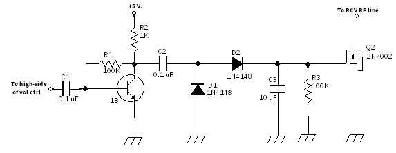
This simple project uses a single stage amplifier to tap into the audio at the input of the volume control, rectify it to a DC level, filter it, and use it to control a MOSFET as a shunt across the receive RF path. This project assumes that you have already installed the RF gain control described here (for the BITX40 or here (for the uBITX) and bridges across it at the control potentiometer.
R3 and C3 are used to not only filter out the audio component, but to form a “fast attack, slow release” control signal. That means that, when a strong signal appears, RF gain will be quickly reduced but will take a second or so to restore to full gain after the signal stops. This avoids “pumping” during a single sideband transmission but is fast to react to very loud signals.
Nearly any general purpose NPN bipolar junction transistor will work as Q1 as long as it has a beta of more than 100. 2N2222, 2N3904, etc. will work quite well. Q2 can be a 2N7000 or a BS170. None of the component values are critical. The 5 volt supply makes it easy to use any part with more than a working limit of just 6 volts and the current drain is low enough to be negligible.
I have found that most 2N7002 transistors will yield at least 20 dB of RF attenuation across the HF spectrum at 50 ohm impedance. Attenuation begins around 1.4 volt bias on the gate referenced to the source and provides maximum action at around the 3.7 volt level. Very effective for a single, simple, and inexpensive device. A great first step.
A more fulsome article with construction details (using surface mount components) is posted on nd6t.com.
This simple circuit led to a discussion on the BITX20 IO Group list, started by Jerry KE7ER, about the BAP64Q pin diode attenuator. This gives 60dB of dynamic range: https://groups.io/g/BITX20/message/32066
Attenuating back in RF gets around the limited dynamic range that Henning points out in the first post of that thread. Note that the control voltage is inverted with respect to the 2n7002 FET, higher voltages give less attenuation. You could get a slightly lower noise figure for the receiver if the attenuator was inserted at a later stage of the RF chain.
Jerry observes, “The BAP64Q is relatively expensive at $0.50 single piece,
the frugal among us will note it’s down at $0.20 if you buy a few thousand.
Mouser and Digikey both stock it, Mouser points you to the wrong BAP64* datasheet. There are other similar small signal pin diode attenuators out there from other manufacturers.”

