
Don ND6T has been tinkering with AGC mods, and has come up with a new solution that gives much high levels of RF compression.
The µBITX presents some challenges with RF AGC system design: There is no RF preamplifier to use as a voltage-controlled attenuator, it is broadband and includes no tuned circuits in the receive path, and the intermediate frequency amplifiers are not configured for variable gain.
If we try to use a PIN diode in the RF, the high insertion loss raises the receiver over-all noise figure appreciably and the driver circuitry begins to become complex. The diode array also necessitates a fair additional current drain.
Original solution
Don’s original solution, designed for the BITX40, was to use a 2N7002 MOSFET as a shunt from RF to ground. The advantages were the simple circuit, the low current drain, and no insertion loss. The disadvantage was the limited dynamic control range (about 20 dB ). This was primarily due to the finite series resistance of the MOSFET when it was driven to full conduction, about 5 ohms. You can see this project by clicking here.
Putting another FET in series
Numerous experiments revealed that adding another 2N7002 in series with the receive RF path made it possible to add another 20 dB (or so) dynamic range across the HF spectrum. This was controlled with the same control bias as the original but the configuration requires driving the source connection of the transistor with the control and biasing the gate at 2.5 volts so that, at idle, the series transistor is driven to full conduction. This control topography requires that the new series transistor to be DC blocked from the RF line.
Pre-requisite Mod
This project assumes that you have already installed the manual RF Gain Control modification since it requires that the trace between relay K1 and relay K3 be cut. I designed mine to simply be glued on the back of the control potentiometer and cut the single-sided un-etched printed circuit board stock to be about 20 mm by 13 mm. The thickness of the completed circuit is only 3 mm and so fits easily.
Theory
Detected audio from the receive audio pre-amplifier is sampled by bringing a twisted pair of wires from the volume control. Just attach the pair across the outside terminals of the control, attaching the wire from the “hot” terminal (which also attaches to “audio1” plug on the main board, pin 4) to the vacant side of C1 on the new board. The other wire attached to the “cold” terminal (which also attaches to pin 3 of the “audio1 plug) connects the the “GND” area of the new board.
This audio sample is then amplified by Q1 and fed through C2 to be rectified by diodes D1 and D2 and filtered by C4 to become the AGC control bias. Signals below 30 millivolts RMS leaves the circuit idle, with Q2 (the series element) biased to full conduction and only adds about 0.6 dB of loss. Q3 (the shunt element) is biased to cutoff and has no effect on the receive signal. Louder signals (S9 and above) create higher bias voltages until maximum is reached (about 1 volt RMS audio) at about 3 volts DC control bias. At this point attenuation is about 50 dB at 3.5 MHz, 34 dB at 30 MHz.
The time constant of C4 and R6 sets the “AGC release” rate, several seconds from full to idle. Charging time is fast, milliseconds, so that sudden strong signals are handled without discomfort. This ratio prevents oscillation and diminishes “pumping” on strong signals. For faster recovery rates, decrease the resistance value of R6. Values down to 100 K work satisfactorily but 1 megaohm worked the best for me.
Construction
A hobby knife was used to isolate the connection pads as shown in the sketches. The remaining copper is then lightly tinned. Resistance checks should then be made to insure that there are no copper scraps or solder bridges between the lands.
I often find it convenient to simply begin in the top right corner of a board and work my way down and left so that I avoid working over previously completed circuit areas. Just place a component, hold it down, and touch the soldering iron to the board near one of the component leads. The thin solder will make a weak attachment to the component (called “tacking”). The builder can then move to another connection on that part and properly solder it using a hand to hold the solder. Then the rest of the component is soldered properly and the value checked with metering to assure a good connection and that the part wasn’t damaged in the process.
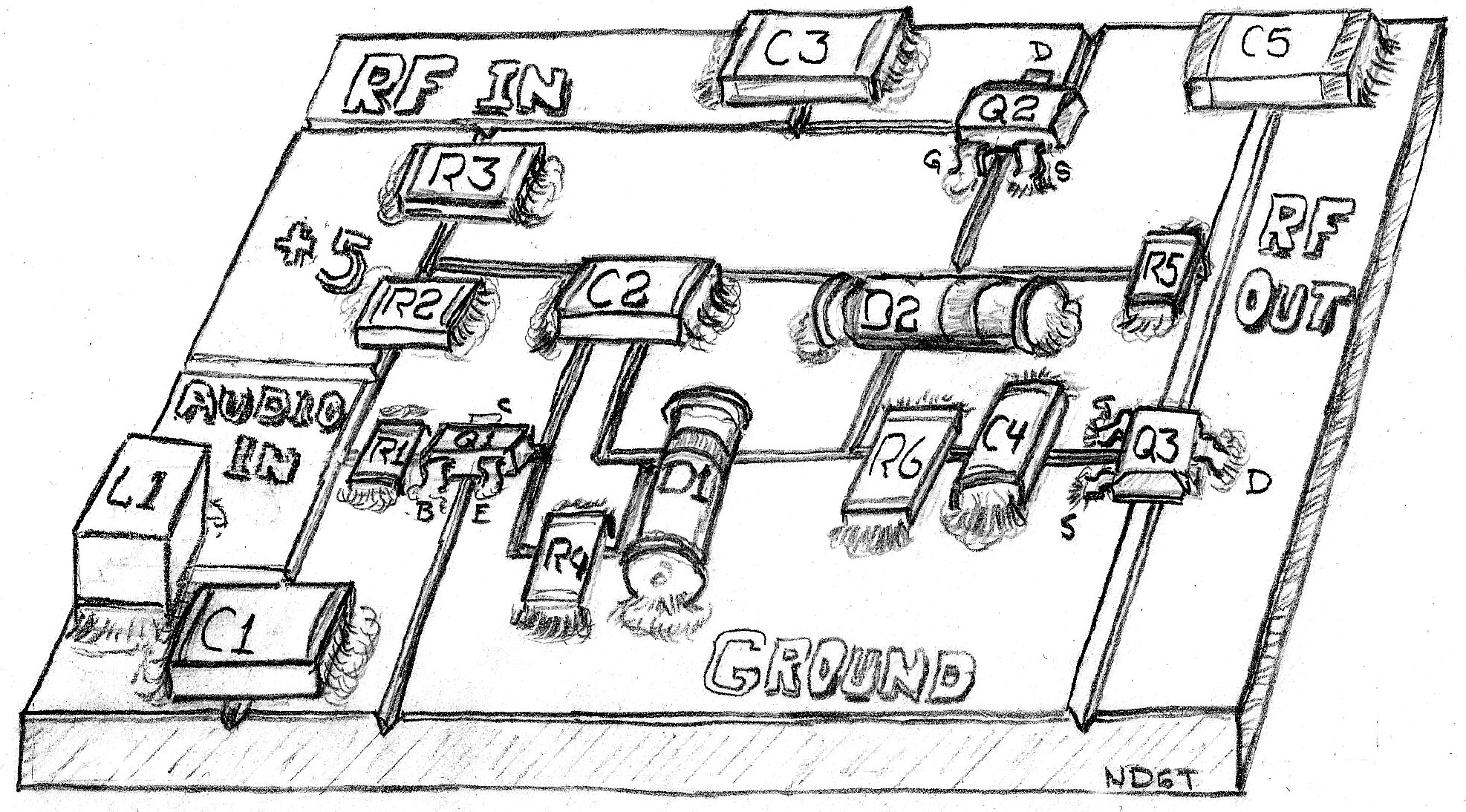
A spot of fast-setting glue holds the board to the back of the manual RF gain control. Remove the coax center conductor from the potentiometer wiper and connect it to the junction of Q3 drain and C5. Run a jumper from the wiper lug of the gain control and connect to the vacant pad of C3. Leaving the manual RF gain control in place will give you extra control should you wish it. Very short jumpers keep things solid and have purer control. Power can be supplied from any nearby 5 volt source (like pin 3 up on the Raduino, usually green wire). It just needs to be from 4 to 5 volts and only draws less than 2 milliamps.
If you want to add a switch to shut off the AGC, do so at the audio input. I would suggest a single-pole double-throw switch with the connection to C1 at the center, ground to one side, and the other to the hot side of the volume control. If power is removed from this circuit Q2 will not be biased “on” and will reduce signal levels significantly.
A good, solid ground is most important. I recommend a ground lug on the potentiometer shaft or on any other nearby ground point. A poor RF ground will yield poor attenuation. 40 dB is a ratio of 1 to 10,000! Hundredths of an ohm count.
If you don’t use an RF gain control
If you don’t have room for a manual RF gain control or a switch there is no reason to worry. This circuit can be left active and placed near the RF path connector without a problem. You could easily build this as a module that simply plugs into the connector. The most critical junction would again be a nearby ground but a third pin, this time through the board to the ground plane, would help. There should be little need to operate without it. If you need to run any tests that need it disabled, just remove the plug to the RF receive path and replace it with a shorting plug across the two RF pins.
If you adverse to surface mount construction, there is little problem in building it with leaded components. Use 2N7000 or BS170 MOSFETs and a 2N3904 or 2N2222 type NPN transistor. Try to keep wiring short and compact in the RF attenuator portion but the rest is very non-critical. If you use an electrolytic or tantalum capacitor for C4, observe polarity.
Parts List
- 1: NPN switching transistor (1B, 2N3904, 2N2222) [Q1]
- 2: N-channel enhancement mode MOSFET (2N7002, 2N7000, BS170) [Q2,3]
- 2: Silicon switching diodes (1N4148, 1N914) [D1,2]
- 2: 0.01 uF, 6 volt or higher ceramic capacitor [C3,5]
- 2: 0.1 uF, 5 volt or higher ceramic capacitor [C1,2]
- 1: 10 uF, 6 volt or higher ceramic (preferred) electrolytic, or tantalum capacitor [C4]
- 1: 1 Kohm resistor [R2]
- 4: 100 Kohm resistor [R1,3,4,5 ]
- 1: 1 Mohm resistor [R6} (or other value, depending upon desired AGC recovery rate)
Explanation
Signals below 50 microvolts (S9) are unaffected. Above that level, the AGC begins to engage. Q2, the pass transistor, begins to turn off a bit while Q3, the shunt transistor, begins to turn on. Signals are attenuated to where the audio output is held to reasonable levels and the rest of the receiver does not experience distortion. If you are considering adding an S meter this circuit may be to advantage due to the amplifier stage. The control bias is available at the junction of D2,C4, Q2,R5 and R6. This is the spot that you would use for a metering source.
Conclusion
AGC makes for a much more pleasurable experience. Don seldom needs to reach for the RF gain control or the volume when an especially strong signal suddenly appears. During nets I can now wander about the shack and still hear all of the check ins. Round tables don’t require a hand on the controls. Things are getting easier.
Recommended by others
Tim AB0WR says, “I am using this new AGC circuit. It works well. You still get a slight pop when an extremely strong signal first comes on but it is very short and, to me at least, not annoying at all. You may want to lower the 1 M Ohm resistor to something smaller to decrease the pop i.e. decrease the attack time. The next time I open the case I’m going to try 500K.”
Jim W0EB says “Thanks ND6T for a very workable AGC circuit!”.
It is clear that this has become the new ubitx.net recommended AGC mod.


