Evening up power output on high bands

Howard WB2VXW received his µBitx, assembled it, and started testing.  He performed a number of modifications to the µBITx in his lab before moving it to its permanent home in the shack.

In particular, he modified the transmitter to improve output power at the higher frequencies. The power out in the original state is about 3 watts at 28 MHz.  His modification brings the power at 28 MHz up to 7 watts on both the 15 and 10 meter bands. On his board, there was not enough range in VR1 to increase the power to anywhere near this level without modification. The other bands remain unchanged in output, at around 11 watts.  The output stage could be modified as others have done by changing the FETs and transformer to improve this further, but Howard was happy with the improvement for now.  He plans on adding a power amplifier later, something between 50 and 100 watts.

Howard’s fix involves adding 3 passive parts:

  • 33 uH inductor in series with R86. I lifted the resistor mounting it on one pad standing up, and teepeeing the inductor between the top of the resistor and the other pad.
  • Adding a 270 pF capacitor across both R87 and R88.

The values are not very critical, I calculated that I needed 27 uH and 220 pF, but the values I tried were in the lab.

The theory is very simple. The closed loop gain of Q911 and Q912 is set by the ratio of R86/R85, or a gain of 10. Adding an inductor into the path in the feedback loop increases the effective impedance at higher frequencies, adding “peaking” to the circuit, thus making the closed loop gain higher.

I think the poor frequency response is in the transformer as well as the transistors Hfe falling to under 25 typically at 30 MHz.  The open loop gain is also increased by bypassing the emitter resistors for higher frequencies.

The transformer is a 2 to 1 step down, (it looks like a trifilar winding) so the theoretical gain of the stage is 5.

Offer of parts

Howard also made a generous offer to  anyone wanting to try the fix and needs the parts.  He has a full reel of each of the parts (2x 270pF capacitor and 33µH inductor), so just Howard a stamped self addressed envelope, and he will send it to you by return mail. The offer is good until he runs out of parts.

Others try it on

Joel N6ALT completed the mod not long after it appeared on the BITX20 IO Groups list with spectacular results. Before the mod he had only 300mw at 13V on 28.500.  After the mod he had 3.8 watts, and after increasing the drive slightly, he now has 4.5 watts. All of the other bands also benefited from the mod.

Tim AB0WR also tried the mod, winding an FT37-43 ferrite to get 33uh. Not as neat as an smd inductor but he didn’t have any in the shack!

Reference

Separating your display from the main board

Gordon W2TTT asked on the BITX20 Group list, “Does anyone have some links to the display/ Raduino extension cable parts?  I want to remote the display from the main board.”

If you want to separate your display from the main board, you should separate the display from the rest of the raduino and plug the “arduino nano” bit into the connector on the main board.  The reason for this is that you don’t want long leads spraying RF around from the oscillator outputs from the si5351a.  This is a sure recipe for birdies in your RX.

Use Dupont connectors (Male to Female) to do this.  Most will find either 10cm or 20cm connectors are suitable.

Jack W8TEE  comments “Jumper wires (aka Dupont wires) are great for breadboarding and experimenting, but my experience is that some of them don’t make a solid connection after recycling (connect/disconnect) a few times. We were getting a lot of noise on a TFT display line and finally tracked it to a faulty Dupont. The Chinese imports seem especially susceptible. If you experience noise or hashing on a display or in the audio, this would be one of the first places I’d look.”

Reference

New AGC system

Don ND6T has been tinkering with AGC mods, and has come up with a new solution that gives much high levels of RF compression.

The µBITX presents some challenges with RF AGC system design: There is no RF preamplifier to use as a voltage-controlled attenuator, it is broadband and includes no tuned circuits in the receive path, and the intermediate frequency amplifiers are not configured for variable gain.

If we try to use a PIN diode in the RF, the high insertion loss raises the receiver over-all noise figure appreciably and the driver circuitry begins to become complex. The diode array also necessitates a fair additional current drain.

Original solution

Don’s original solution, designed for the BITX40, was to use a 2N7002 MOSFET as a shunt from RF to ground. The advantages were the simple circuit, the low current drain, and no insertion loss. The disadvantage was the limited dynamic control range (about 20 dB ). This was primarily due to the finite series resistance of the MOSFET when it was driven to full conduction, about 5 ohms. You can see this project by clicking here.

Putting another FET in series

Numerous experiments revealed that adding another 2N7002 in series with the receive RF path made it possible to add another 20 dB (or so) dynamic range across the HF spectrum. This was controlled with the same control bias as the original but the configuration requires driving the source connection of the transistor with the control and biasing the gate at 2.5 volts so that, at idle, the series transistor is driven to full conduction. This control topography requires that the new series transistor to be DC blocked from the RF line.

Pre-requisite Mod

This project assumes that you have already installed the manual RF Gain Control modification since it requires that the trace between relay K1 and relay K3 be cut. I designed mine to simply be glued on the back of the control potentiometer and cut the single-sided un-etched printed circuit board stock to be about 20 mm by 13 mm. The thickness of the completed circuit is only 3 mm and so fits easily.

Theory

Detected audio from the receive audio pre-amplifier is sampled by bringing a twisted pair of wires from the volume control. Just attach the pair across the outside terminals of the control, attaching the wire from the “hot” terminal (which also attaches to “audio1” plug on the main board, pin 4) to the vacant side of C1 on the new board. The other wire attached to the “cold” terminal (which also attaches to pin 3 of the “audio1 plug) connects the the “GND” area of the new board.

This audio sample is then amplified by Q1 and fed through C2 to be rectified by diodes D1 and D2 and filtered by C4 to become the AGC control bias. Signals below 30 millivolts RMS leaves the circuit idle, with Q2 (the series element) biased to full conduction and only adds about 0.6 dB of loss. Q3 (the shunt element) is biased to cutoff and has no effect on the receive signal. Louder signals (S9 and above) create higher bias voltages until maximum is reached (about 1 volt RMS audio) at about 3 volts DC control bias. At this point attenuation is about 50 dB at 3.5 MHz, 34 dB at 30 MHz.

The time constant of C4 and R6 sets the “AGC release” rate, several seconds from full to idle. Charging time is fast, milliseconds, so that sudden strong signals are handled without discomfort. This ratio prevents oscillation and diminishes “pumping” on strong signals. For faster recovery rates, decrease the resistance value of R6. Values down to 100 K work satisfactorily but 1 megaohm worked the best for me.
Construction

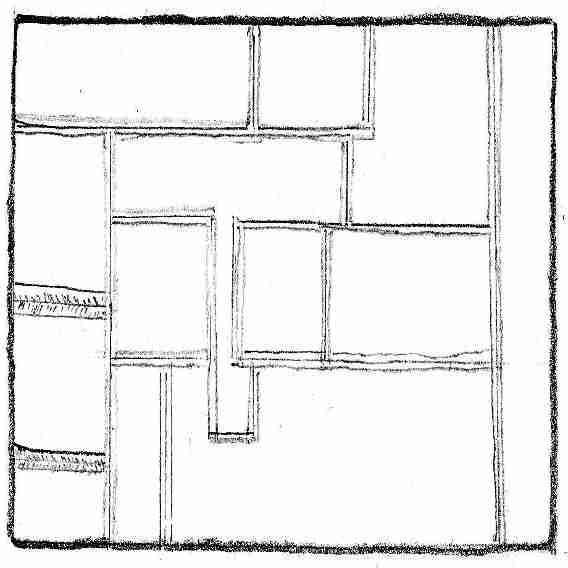
A hobby knife was used to isolate the connection pads as shown in the sketches. The remaining copper is then lightly tinned. Resistance checks should then be made to insure that there are no copper scraps or solder bridges between the lands.

I often find it convenient to simply begin in the top right corner of a board and work my way down and left so that I avoid working over previously completed circuit areas. Just place a component, hold it down, and touch the soldering iron to the board near one of the component leads. The thin solder will make a weak attachment to the component (called “tacking”). The builder can then move to another connection on that part and properly solder it using a hand to hold the solder. Then the rest of the component is soldered properly and the value checked with metering to assure a good connection and that the part wasn’t damaged in the process.
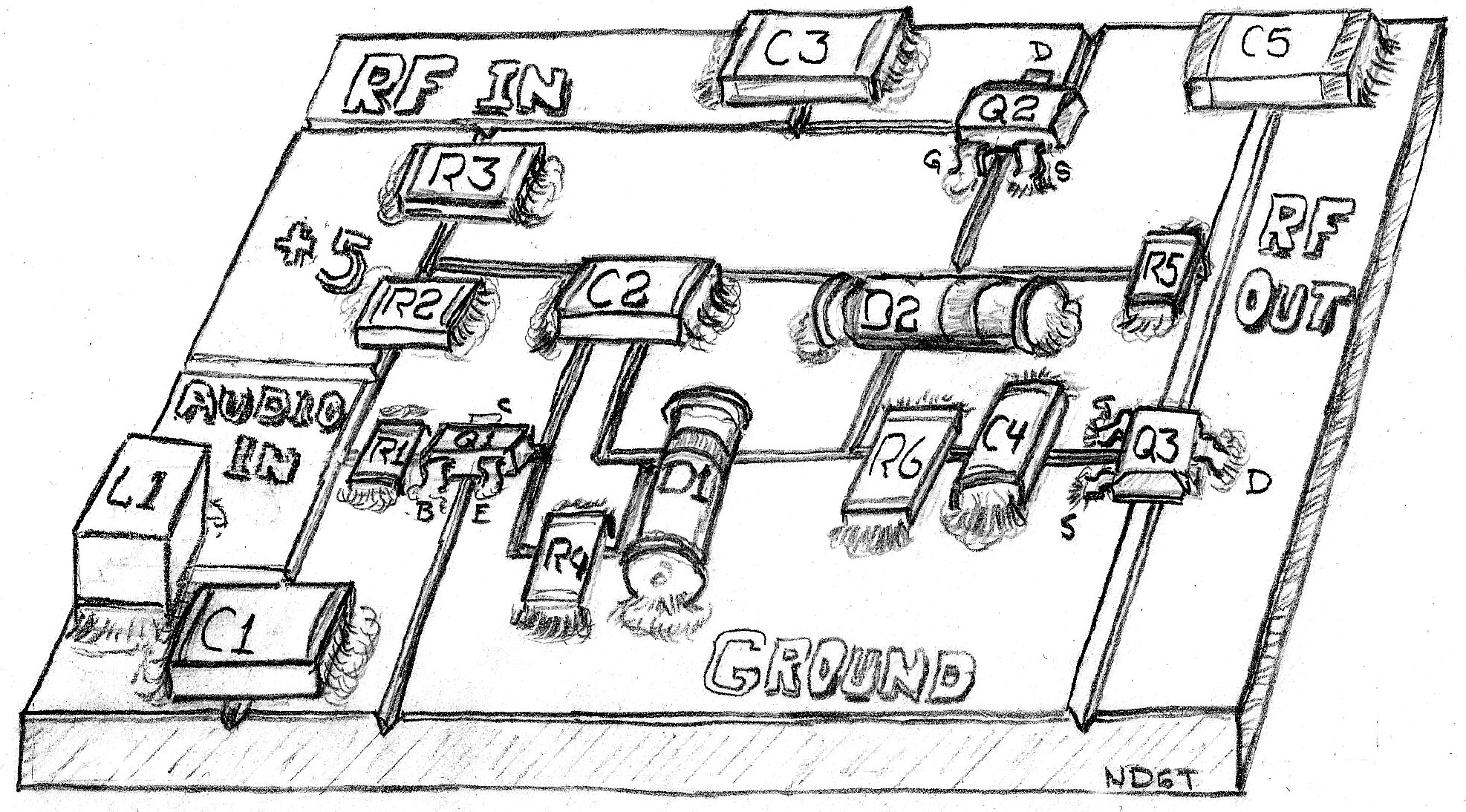


A spot of fast-setting glue holds the board to the back of the manual RF gain control. Remove the coax center conductor from the potentiometer wiper and connect it to the junction of Q3 drain and C5. Run a jumper from the wiper lug of the gain control and connect to the vacant pad of C3. Leaving the manual RF gain control in place will give you extra control should you wish it. Very short jumpers keep things solid and have purer control. Power can be supplied from any nearby 5 volt source (like pin 3 up on the Raduino, usually green wire). It just needs to be from 4 to 5 volts and only draws less than 2 milliamps.

If you want to add a switch to shut off the AGC, do so at the audio input. I would suggest a single-pole double-throw switch with the connection to C1 at the center, ground to one side, and the other to the hot side of the volume control. If power is removed from this circuit Q2 will not be biased “on” and will reduce signal levels significantly.

A good, solid ground is most important. I recommend a ground lug on the potentiometer shaft or on any other nearby ground point. A poor RF ground will yield poor attenuation. 40 dB is a ratio of 1 to 10,000! Hundredths of an ohm count.

If you don’t use an RF gain control

If you don’t have room for a manual RF gain control or a switch there is no reason to worry. This circuit can be left active and placed near the RF path connector without a problem. You could easily build this as a module that simply plugs into the connector. The most critical junction would again be a nearby ground but a third pin, this time through the board to the ground plane, would help. There should be little need to operate without it. If you need to run any tests that need it disabled, just remove the plug to the RF receive path and replace it with a shorting plug across the two RF pins.

If you adverse to surface mount construction, there is little problem in building it with leaded components. Use 2N7000 or BS170 MOSFETs and a 2N3904 or 2N2222 type NPN transistor. Try to keep wiring short and compact in the RF attenuator portion but the rest is very non-critical. If you use an electrolytic or tantalum capacitor for C4, observe polarity.

Parts List

  • 1: NPN switching transistor (1B, 2N3904, 2N2222) [Q1]
  • 2: N-channel enhancement mode MOSFET (2N7002, 2N7000, BS170) [Q2,3]
  • 2: Silicon switching diodes (1N4148, 1N914) [D1,2]
  • 2: 0.01 uF, 6 volt or higher ceramic capacitor [C3,5]
  • 2: 0.1 uF, 5 volt or higher ceramic capacitor [C1,2]
  • 1: 10 uF, 6 volt or higher ceramic (preferred) electrolytic, or tantalum capacitor [C4]
  • 1: 1 Kohm resistor [R2]
  • 4: 100 Kohm resistor [R1,3,4,5 ]
  • 1: 1 Mohm resistor [R6} (or other value, depending upon desired AGC recovery rate)

Explanation

Signals below 50 microvolts (S9) are unaffected. Above that level, the AGC begins to engage. Q2, the pass transistor, begins to turn off a bit while Q3, the shunt transistor, begins to turn on. Signals are attenuated to where the audio output is held to reasonable levels and the rest of the receiver does not experience distortion. If you are considering adding an S meter this circuit may be to advantage due to the amplifier stage. The control bias is available at the junction of D2,C4, Q2,R5 and R6. This is the spot that you would use for a metering source.

Conclusion

AGC makes for a much more pleasurable experience. Don seldom needs to reach for the RF gain control or the volume when an especially strong signal suddenly appears. During nets I can now wander about the shack and still hear all of the check ins. Round tables don’t require a hand on the controls. Things are getting easier.

Recommended by others

Tim AB0WR says, “I am using this new AGC circuit. It works well. You still get a slight pop when an extremely strong signal first comes on but it is very short and, to me at least, not annoying at all. You may want to lower the 1 M Ohm resistor to something smaller to decrease the pop i.e. decrease the attack time. The next time I open the case I’m going to try 500K.”

Jim W0EB says “Thanks ND6T for a very workable AGC circuit!”.

It is clear that this has become the new ubitx.net recommended AGC mod.

Reference

Baofeng Speaker/Mics and uBITx

There has been a bit of discussion on the BITX20 Groups IO list about Baofeng mics, mods required to work with the µBITx, and what to do about a mic jack. This article tries to sum up thoughts on using the Baofeng mic.

Basics

The Baofeng Speaker/Mic can be obtained very cheaply, either direct from China (e.g. on Aliexpress.com or Banggood.com, or eBay.com) or via third parties in your country.   Be warned that almost none of these will be a genuine Baofeng mic.  There are many different varieties of “knock-off”, and they are of very varying quality.   However, most are adequate for µBITx use.

The wiring in the microphone is not standardised (i.e the colour of the wires varies).  In some cases the wiring simply doesn’t work.  In this instance, you should throw away the Speaker-Mic as the wiring is non-repairable.   Buy several to safeguard against the odd one that has wiring issues.

The microphone element is so-so, you can replace the one in the Speaker/Mic with the element that comes with the kit as required.  You may also need to drill out the tiny hole to be a bit bigger to make a reasonable air passage to the element.   The speaker is not high quality and will not give much volume.   When using the speaker-mic in the µBITx, most of us don’t use the speaker at all.

Standard wiring will work on the BITx40, and the LED in the Speaker/Mic will even light up.  It won’t on the µBITx, because the PTT line works differently.  This is connected to +5v from an arduino line (messing up the bias on the microphone).

Disassemble the mic, and rewire (using a multimeter to test connections) so that the PTT switch is wired separately from the microphone element.  You can use a common ground return for the mic, speaker and PTT.  See the original circuit diagram for the speaker/mic here.

Panel jack mounting

A key question that those with a Baofeng Speaker/Mic, is whether you should retain the 3.5mm and 2.5mm plug, or cut it off.

John KG5WJQ observes that they sell a combined jack on Alibaba and the price is fine.  The problem is that it is a PCB mount jack so that can result in some difficulties with mounting the jack in a case.

Craig KM4YEC uses panel mount mono jacks, one 3.5″ and one 2.5″, sourced from Radio Shack in store stock (but they could probably be ordered online).  He says,  “If you turn these back to back, and butt them against each other, with the ears turned out, it is a perfect fit for spacing.”   

Craig uses only the PTT, and the Mic element in the enclosure.  He enlarges the hole in front of the element, removes the speaker, and makes sure the only two circuits are PTT and Mic.  He went as far as removing all the SMD components and unnecessary trace runs using exacto knife cuts.

Glenn VK3PE fitted standard 3.5 and 2.5mm jacks at the rear of his uBITX build. NOTE the 3.5mm jack needs to be insulated from the chassis to work as the PTT is connected to what is normally ‘ground’ on a stereo socket. Glenn used some plastic washers to insulate it.

The challenge with this approach is that the spacing between the two jacks needs to be reasonably precise.

There is nothing to stop you from cutting off the plug and wiring it directly into the circuit.  This is a cheap option (no plug and socket required), but is a bit inconvenient when it comes to moving the rig, as the microphone is permanently attached.

The other option is to remove the plug altogether and use different connectors.   Many constructors like to use a standard 4 pin mic jack or similar style 8 pin jack used by the big three Japanese amateur rig manufacturers as illustrated below:

Mike ZL1AXG uses Kenwood wiring on a standard 8 pin mic connector as shown below.

Is there a better choice of microphone?

Dave K8WPE felt his Baofeng speaker mike was of such poor quality that he went ahead and bought an almost identical microphone from Btech.  This is a QHM22, a much better product, for US$23.00.  The speaker is top notch and reports of his voice quality are also very good. So the Btech mike might be a better choice.

Reference

Flatten the power curve and set your power out in software

John VK2ETA  has some pretty good ideas. A few days ago he worked on an AGC system using the first IF stage (at 45MHz) to control gain at the front end of the system.   He has now got some pretty good results using a limited amount of memory in the firmware to flatten out the power curve on transmit.  At this stage it only works in voice and digital modes (LSB and USB). Because CW is achieved by unbalancing the first mixer after the IF filter, this approach will not work on CW.

By shifting the IF frequency on the filter, John is able to produce a fixed attenuation that keeps the output power within the required limits.

The process is two fold:

  • a one off calibration exercise.
  •  a menu item that selects Low, High or Max power.

John has used 5W and 10W as targets for the Low and High values.

His results (remembering he has modified the final stage with RD16s and a number of other changes have been made to his transceiver):

  • 80m to 10m in low power settings have variations between 4 and 6 watts.
  • 80m to 10m In the high power setting has a range between 9 and 11 watts.
  • Only 16 bytes of data points are required (could be stored in EEPROM if desired).

His ATU uses a 2nd Arduino.   He has used a spare digital output to send a 1500Hz tone, low-pass filtered, to the microphone input for calibration purposes.  The audio filtering plus the 2nd IF filter take care of the audio harmonics and the signal is clean. This could be done in the Raduino if digital lines are freed up, such as by using an I2C display.

The tone also provides a tune up facility in low power.

He can transmit in digital modes in low power mode without having to adjust the drive every time he changes bands.  Perfect!

John will update the code in the file section so that others can incorporate this new feature into their firmware if they desire.

John acknowledges Jerry KE7ER’s idea of using fixed tables to perform the High/Low calibration function.

Firmware uploaded to files area

John has uploaded an update of the KD8CEC based software (V1.04 based) for Raduino and ATU Arduino.

Key changes in Version 20180411:

– Made the menu system dynamic so that items can be inserted at compile time or can be context-dependant at run time.
– Added output power attenuation for 80 to 10M using first IF shift.
– Added new menu item “Power Level”: low/high/max for SSB modes.
– Made CW menu items display dependant on having CW modes selected.
– Reduced the level at which the software AGC comes in. Adjusted the correction of S-Meter when software AGC comes into play.
– Changed tone generation for ATU tuning sequence from CW to using SSB with the 2nd Arduino generated tone.
– Change tune sequence to

a)Select the “Low” power setting before performing a tune and
b)Change tune frequency to tune on carrier (offset by audio tone frequency).

Assumes the following hardware change (only if using an ATU): a digital output on the ATU Arduino is used to generate a tone. An audio filter identical to the Raduino CW audio tone filter is used and it’s output is connected to the mic input of the SSM2167 module. If digital outputs are freed-up on the Raduino, for example by using an I2C display, the same can be implemented with only the Raduino.

This allows a low power tune function.

Reference

Glenn VK3PE has built up one of the 9 component anti thump circuits described by ND6T (but it is in fact a design by VA7AT ).  He has yet to actually try it in his rig.

The PCB is about 26 x 10mm in size. Only difference to ND6T’s version is he placed the 10uF’s on the PCB also. ie remove from uBITX board and fit to this board. Otherwise it follows ND6T’s web page for installation. It is made from SMD 0805 parts.

Reference

Converting to an I2C display and other developments

Ian KD8CEC is busy opening up the possibilities for including different code sections in his new version 1.07 under development.  This will include the ability to readily shift to an I2C display in order to reclaim digital I/O ports needed for other features.

In the mean time, Bill K9HZ provides a succinct code listing required to get an I2C display to work

The following TWO things need to be done in Ian’s version 1.07 code (BETA):

1. Change Display models in “ubitx_20” :

From this:

#define UBITX_DISPLAY_LCD1602P      //LCD mounted on unmodified uBITX

//#define UBITX_DISPLAY_LCD1602I    //I2C type 16 x 02 LCD

//#define UBITX_DISPLAY_LCD2404P    //24 x 04 LCD

//#define UBITX_DISPLAY_LCD2404I    //I2C type 24 x 04 LCD

To this:

//#define UBITX_DISPLAY_LCD1602P    //LCD mounted on unmodified uBITX

#define UBITX_DISPLAY_LCD1602I        //I2C type 16 x 02 LCD

//#define UBITX_DISPLAY_LCD2404P    //24 x 04 LCD

//#define UBITX_DISPLAY_LCD2404I    //I2C type 24 x 04 LCD

2. Update Ian’s code to use the I2C libraries in “ubitx_lcd_1602i” :

From this:

#include <LiquidCrystal.h>

LiquidCrystal lcd(8,9,10,11,12,13);

To this:

#include <LiquidCrystal_I2C.h>

LiquidCrystal_I2C lcd(0x3F, 2, 1, 0, 4, 5, 6, 7, 3, POSITIVE);  //

JUST MAKE SURE THE ADDRESS IS CORRECT…

in the instance above the add-on board on the back of the display is set to address “3F”.  You can use the scanner to find the correct address.

Reference


Using 2nd channel of TDA2822 for S-meter

John VK2ETA suggests using a section of the original AGC circuit of the µBITx (design by Ashhar Farhan VU2ESE) for generating a signal for an S-meter so that this can be used by his modified software.

This was part of the pre-production uBitx diagram but was not implemented in the production version.

The 2N7002 is used as an automatic gain control and can be used or not for that application.   The circuit has limitations since it was not included in the production version.

You would need to insert a trim-potentiometer (10K ohms is good) between pin 6 of the TDA2822 and the VOL-H connection to adjust the sensitivity, plus (VERY IMPORTANT) a voltage divider, between the cathode of the diode and the ground, to limit the voltage to under 5VDC for the analogue input of the Raduino.

John would use 330K ohm in series with 100K ohm to the ground, and connect A7 to the junction of the two resistors.

Further adjustments are available in the software if required as we define the 9 stages of the S-meter display (first stage is zero, then 6 stages for growing bars, 1 stage showing “+” and one stage showing the custom “++” symbol). In ubitx_20.ino it shows as:

int sMeterLevels[] = {0, 5, 17, 41, 74, 140, 255, 365, 470};

The values in the array are the measured values on the analogue input (defined as A7 above) at which we step into a higher “stage” and can go from zero for zero volts to 1023 for a 5V DC value.

Reference

Using a 1N4004 or similar as a varicap or pin diode for AGC control

Allison KB1GMX finds it  odd that every one seems to be bent on levelling the audio volume in the audio circuit.

The Bitx or uBitx has enough gain and handy places that RF gain control based on audio detection works very well. The easy way is replace R13 (ubitx) with a diode such as 1n400x (x=1 to 7) and controlling the  current through the diode to make it behave as a variable resistance at RF.

The current would be about 4-6ma at max gain and decrease to zero (0) at minimum gain.  For that design the AGC range is about 26 to 32db depending on the band. If you feel that is not enough AGC range then add the same mod at R33 and with both the AGC range is near 60+ DB, generally enough.

AGC in this form is less prone to overload distortion as you are lowering gain. The control could be a pot between 8V (or RX-V) and ground and a series 1K resistor to the diode (x2 if using both diodes). That gives a manual gain control. To make it automatic use a circuit to detect the voltage at the top of the audio gain pot and feed that voltage to the gain control diodes. The circuit should be arranged to put 4-8V out at NO Audio and decrease to zero volts with increasing audio.

The 1n400x series with minor reservations makes a fine substitute for a PIN diode, the preferred but more costly device for this function. Beside being widely available and cheap  makes it useful.  It also makes a good 20pf varicap and a 1A rectifier to 1000V (1n4007).

This was tested on the first bitx20 that Allison built over a decade ago to test AGC.  It has been used on several older Tentec radios and more than few of her own design. That said its far from a new idea or design as its documented in EMRFD and an older book (Solid State Design, ARRL press, now out of print).

Jerry KE7ER climbs into the conversation saying:

“I have no idea what the capacitance of a slightly forward biased 1n400x is,
figure 6 here suggests it’s north of 30pf:    Therefore, it might be marginal at 45mhz, and can vary wildly with diode type and brand.

Consensus seems to be that a 1n4007 is preferred over other 1n400x flavors for use as a PIN.   Some experimentation may be required using diodes from different manufacturers:

If you are paying $5 postage to ship in some 1n4007’s, you might consider
also getting some BAP64-02’s at $0.43 each single unit pricing, Mouser 771-BAP64-02-T/R.  These are fully specified for use as an RF PIN diode.

Reference